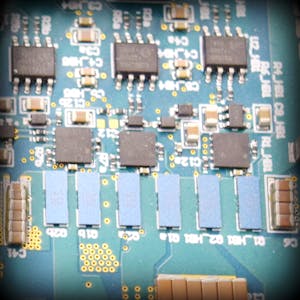
Understanding the Challenges of Driving a Half-Bridge MOSFET
Driving a half-bridge MOSFET configuration is critical in various power electronics applications, such as motor drives, inverters, and power supplies. While half-bridge configurations offer efficiency and performance advantages, they come with their own set of challenges. This blog will delve into these challenges and explore methods to address them.
1. Switching Transients and Noise
One of the primary challenges in driving half-bridge MOSFETs is managing the switching transients and noise. When the MOSFET switches, it generates high-frequency transients due to the rapid voltage and current changes. These transients can cause several issues:
- Electromagnetic Interference (EMI): The rapid switching generates electromagnetic interference, which can affect nearby sensitive circuits.
- Ringings and Oscillations: Inductive elements in the circuit can cause ringing, which leads to voltage spikes that can exceed the MOSFET's voltage rating.
Mitigation Strategies:
- Use of snubber circuits to dampen oscillations.
- Careful PCB layout to minimize inductive loops.
- Gate resistors to control the switching speed and reduce transients.
2. Dead Time Management
In a half-bridge configuration, there are two MOSFETs: one high-side and one low-side. Both MOSFETs should never be on simultaneously, as this would create a short circuit through the power supply, known as shoot-through. To prevent this, a dead time is introduced:
- Dead Time: A short period during which both MOSFETs are off to avoid shoot-through.
Challenges with Dead Time:
- Too short dead time can still cause shoot-through.
- Too long dead time can reduce efficiency as it leads to higher conduction losses.
Mitigation Strategies:
- Precise dead time control using dedicated gate driver ICs.
- Adaptive dead time algorithms that adjust the dead time dynamically based on operating conditions.
3. High-Side Drive Complexity
Driving the high-side MOSFET in a half-bridge configuration is more complex than the low-side because the source of the high-side MOSFET is not at a fixed potential but swings with the output voltage.
Challenges:
- Level Shifting: The gate driver must provide a voltage higher than the source potential of the high-side MOSFET.
- Bootstrap Circuitry: Often used to supply the gate driver with the necessary voltage, but it comes with its own set of challenges like bootstrap capacitor sizing and charging.
Mitigation Strategies:
- Use of isolated gate drivers or gate driver ICs with integrated bootstrap functionality.
- Bootstrap capacitor sizing to ensure it holds enough charge for the duration of the switching cycle.
4. Gate Charge and Drive Power
MOSFETs require a certain amount of charge to switch on and off, known as gate charge. The gate driver must be capable of sourcing and sinking this charge rapidly.
Challenges:
- High Gate Charge: Leads to increased power dissipation in the gate driver and can slow down switching.
- Gate Driver Power: The gate driver must supply sufficient current to switch the MOSFET quickly, which can be demanding, especially at high switching frequencies.
Mitigation Strategies:
- Use gate drivers with high current capability.
- Optimize gate resistance to balance between switching speed and power dissipation.
5. Thermal Management
Switching losses and conduction losses in MOSFETs generate heat. Efficient thermal management is crucial to ensure reliable operation.
Challenges:
- Heat Dissipation: High power dissipation can lead to overheating, reducing the lifespan of the MOSFET.
- Thermal Runaway: Inadequate cooling can cause a positive feedback loop where increasing temperature leads to higher losses and further temperature rise.
Mitigation Strategies:
- Use of heat sinks and thermal interface materials.
- Proper PCB design to enhance heat dissipation.
- Thermal monitoring and protection circuits to prevent overheating.
6. Parasitic Inductances and Capacitances
Parasitic elements in the circuit can significantly affect performance, especially at high frequencies.
Challenges:
- Parasitic Inductance: Can cause voltage spikes during switching transients.
- Parasitic Capacitance: Can lead to increased switching losses and noise.
Mitigation Strategies:
- Minimize loop areas in PCB layout to reduce inductance.
- Use of low-inductance components and layouts.
- Proper component placement to minimize parasitic effects.
Conclusion
Driving a half-bridge MOSFET involves navigating a series of technical challenges, from managing switching transients and ensuring proper dead time to dealing with the complexities of high-side driving and thermal management. By understanding these challenges and implementing appropriate mitigation strategies, designers can optimize the performance and reliability of their half-bridge circuits. Proper component selection, careful PCB layout, and effective thermal management are key to achieving efficient and robust half-bridge MOSFET operation.


No comments